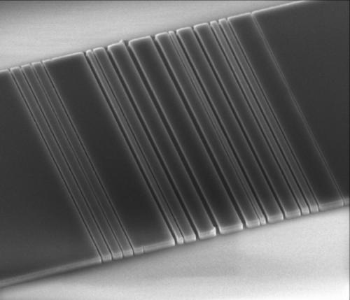
This tiny slice of silicon, etched in Jelena Vuckovic’s lab at Stanford with a pattern that resembles a bar code, is one step on the way toward linking computer components with light instead of wires. Credit: Vuckovic Lab
Stanford engineers have designed and built a prism-like device that can split a beam of light into different colors and bend the light at right angles, a development that could eventually lead to computers that use optics, rather than electricity, to carry data.
They describe what they call an “optical link” in an article in Scientific Reports.
The optical link is a tiny slice of silicon etched with a pattern that resembles a bar code. When a beam of light is shined at the link, two different wavelengths (colors) of light split off at right angles to the input, forming a T shape. This is a big step toward creating a complete system for connecting computer components with light rather than wires.
“Light can carry more data than a wire, and it takes less energy to transmit photons than electrons,” said electrical engineering Professor Jelena Vuckovic, who led the research.
In previous work her team developed an algorithm that did two things: It automated the process of designing optical structures and it enabled them to create previously unimaginable, nanoscale structures to control light.
Now, she and lead author Alexander Piggott, a doctoral candidate in electrical engineering, have employed that algorithm to design, build and test a link compatible with current fiber optic networks.
Creating a silicon prism
The Stanford structure was made by etching a tiny bar code pattern into silicon that split waves of light like a small-scale prism. The team engineered the effect using a subtle understanding of how the speed of light changes as it moves through different materials.
What we call the speed of light is how fast light travels in a vacuum. Light travels a bit more slowly in air and even more slowly in water. This speed difference is why a straw in a glass of water looks dislocated.
A property of materials called the index of refraction characterizes the difference in speed. The higher the index, the more slowly light will travel in that material. Air has an index of refraction of nearly 1 and water of 1.3. Infrared light travels through silicon even more slowly: it has an index of refraction of 3.5.
The Stanford algorithm designed a structure that alternated strips of silicon and gaps of air in a specific way. The device takes advantage of the fact that as light passes from one medium to the next, some light is reflected and some is transmitted. When light traveled through the silicon bar code, the reflected light interfered with the transmitted light in complicated ways.
The algorithm designed the bar code to use this subtle interference to direct one wavelength to go left and a different wavelength to go right, all within a tiny silicon chip eight microns long.
Both 1300-nanometer light and 1550-nanometer light, corresponding to C-band and O-band wavelengths widely used in fiber optic networks, were beamed at the device from above. The bar code-like structure redirected C-band light one way and O-band light the other, right on the chip.
Convex optimization
The researchers designed these bar code patterns already knowing their desired function. Since they wanted C-band and O-band light routed in opposite directions, they let the algorithm design a structure to achieve it.
“We wanted to be able to let the software design the structure of a particular size given only the desired inputs and outputs for the device,” Vuckovic said.
To design their device they adapted concepts from convex optimization, a mathematical approach to solving complex problems such as stock market trading. With help from Stanford electrical engineering Professor Stephen Boyd, an expert in convex optimization, they discovered how to automatically create novel shapes at the nanoscale to cause light to behave in specific ways.
“For many years, nanophotonics researchers made structures using simple geometries and regular shapes,” Vuckovic said. “The structures you see produced by this algorithm are nothing like what anyone has done before.”
The algorithm began its work with a simple design of just silicon. Then, through hundreds of tiny adjustments, it found better and better bar code structures for producing the desired output light.
Previous designs of nanophotonic structures were based on regular geometric patterns and the designer’s intuition. The Stanford algorithm can design this structure in just 15 minutes on a laptop computer.
They have also used this algorithm to design a wide variety of other devices, like the super-compact “Swiss cheese” structures that route light beams to different outputs not based on their color, but based on their mode, i.e., based on how they look. For example, a light beam with a single lobe in the cross-section goes to one output, and a double lobed beam (looking like two rivers flowing side by side) goes to the other output. Such a mode router is equally as important as the bar code color splitter, as different modes are also used in optical communications to transmit information.
The algorithm is the key. It gives researchers a tool to create optical components to perform specific functions, and in many cases such components didn’t even exist before. “There’s no way to analytically design these kinds of devices,” Piggott said.
via phys.org


